Are you curious about ASML’s joint venture partners? Wondering who works alongside this leading technology company to bring groundbreaking innovations to life? Look no further, because I have a comprehensive guide just for you! As someone who has been studying and researching this topic for years, I can confidently provide all the information you need. In this article, we’ll dive into the details of ASML’s joint venture partnerships- from who they are, their roles in the company, and how they contribute to ASML’s success. So let’s explore together and uncover the key players behind one of the most influential tech companies today.
So, who are ASML’s joint venture partner?
ASML’s joint venture partners include major semiconductor companies such as Intel, Samsung, TSMC, and GlobalFoundries. These partnerships are crucial for ASML as they provide the company with access to cutting-edge technology and expertise in the field of chip manufacturing.
Intel is one of ASML’s longest-standing partners, dating back to 1984. They have a strategic collaboration focused on developing advanced lithography systems for next-generation chips.
Samsung joined forces with ASML in 2012 to develop extreme ultraviolet (EUV) lithography technology. This partnership has resulted in significant advancements in chip production and has solidified both companies’ positions as leaders in the industry.
TSMC became a partner of ASML in 1995 and has since collaborated on multiple projects aimed at improving chip manufacturing processes. Their most recent partnership focuses on advancing EUV technology for future generations of chips.
GlobalFoundries partnered with ASML in 2009 to jointly develop new technologies that enable more efficient and cost-effective production of semiconductors. This partnership allows both companies to stay ahead of competitors by continuously innovating and improving their products.
Overall, these joint venture partnerships play a critical role in driving innovation and advancement within the semiconductor industry. By combining resources and expertise, ASML and its partners are able to push boundaries and deliver cutting-edge solutions that shape our modern world.
Understanding Joint Ventures and ASML’s Approach
When you hear the term Joint Venture, what comes to mind? It’s a phrase that rings of business undertakings and corporate collaborations. But, look a bit closer, it is an arrangement where two or more parties agree to pool their resources for accomplishing a specific task, usually within a defined timeframe. This task might be any business project or other commercial activity. With each party contributing equity and sharing in both the profits and losses of the venture – this unique agreement serves as fertile ground for innovation.
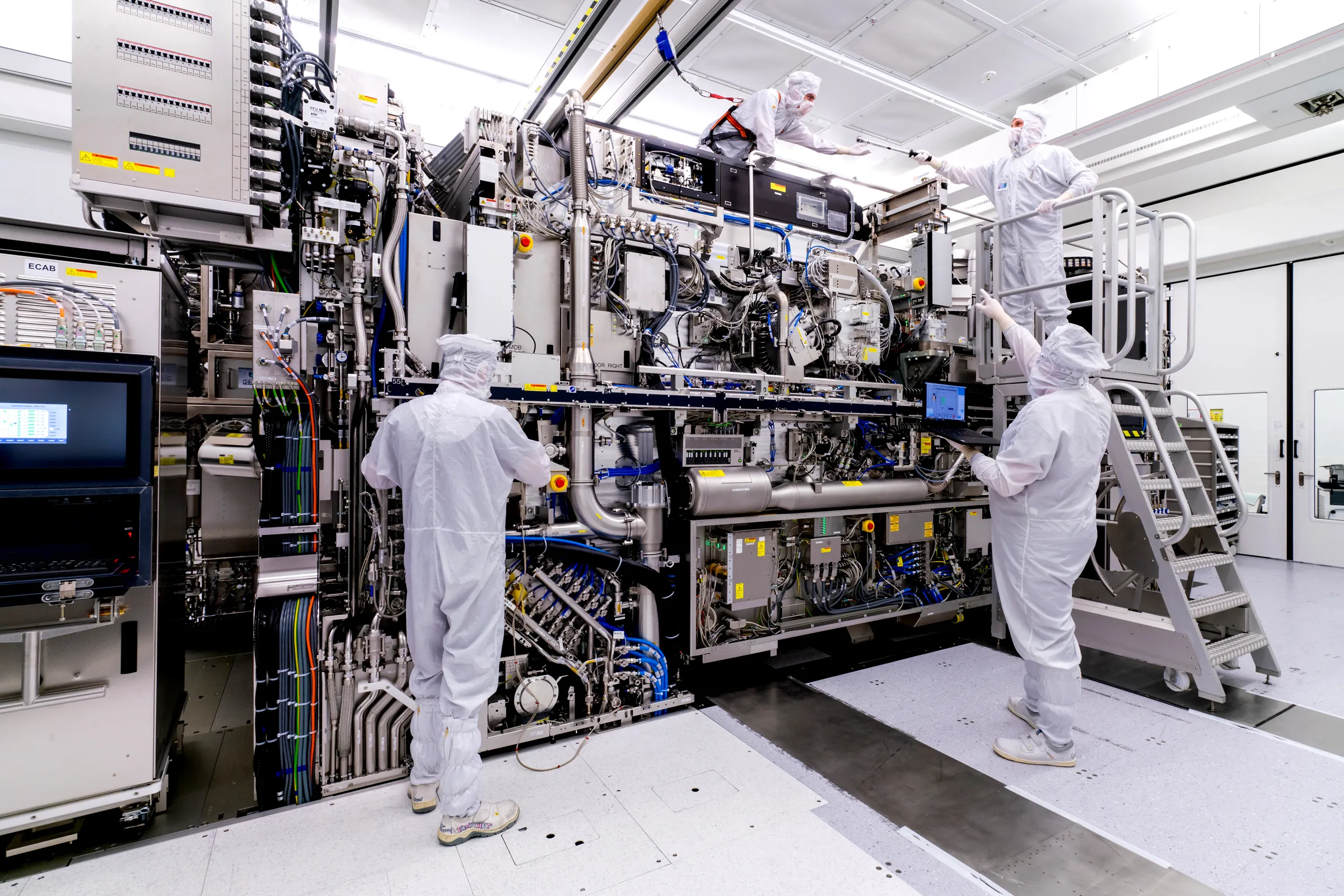
Let’s talk about ASML now. ASML, based out of the Netherlands, is one of those companies that has made joint ventures part of its core operation strategy. They are world leaders in producing photolithography systems used by chipmakers like Intel and Samsung. Rather than going solo on all its operations, it makes strategic partnerships with others thereby incorporating various perspectives into their innovative processes.
- Their approach towards joint ventures takes an inclusive form; they believe diversity fuels innovation.
- They work collaboratively with partners who possess complementary technological capabilities which helps them stay ahead in technology.
- Focusing on collaborative success rather than competitive advantage allows ASML to continually drive industry progress.
Therefore, through these joint ventures, not only does ASML get access to additional resources and expertise but also gains new insights into diverse market trends thereby staying ahead while still remaining true to their vision- ‘Unlocking human potential’.
The Role of Intel in ASML’s Lithography Innovation
The Role of Intel in ASML’s Lithography Innovation is a fascinating tale of technological synergy and cooperative advancement. Did you know that it was Intel, the globally renowned microprocessor producer, who played an instrumental role in catapulting ASML to become the world’s leading lithography innovator? Yes indeed! This collaboration has been vital for both companies, propelling them forward in their respective fields.
Intel saw tremendous potentiality within ASML and made a significant investment to boost its research and development capabilities back in 2012. Through this strategic alliance, ASML acquired not only capital but also access to Intel’s vast reservoirs of expertise. The result? A revolutionary technology known as Extreme Ultraviolet (EUV) lithography was born out of this intellectual collaboration. It changed how semiconductors were manufactured, allowing tech companies to create smaller yet more powerful devices.
- EUV technology brought about increased efficiency
- It led to substantial energy saving
- Revolutionized scalability potentials within miniature device production.
The most remarkable thing about the bond between Intel and ASML is how they have managed to balance competition with cooperation. In essence,the link between these two giants epitomizes what can be achieved when industry leaders work together towards common milestones instead of battling one another all alone.The strides they’ve made together are nothing short of spectacular – setting new benchmarks for others while constantly pushing the envelope on technological possibilities.
Read also: What Amancio Ortega thinks about venture capital
ASML’s Partnership with Samsung: Advancing EUV Technology
The world of technology is forever moving, steadily advancing towards the next best thing. This drive for innovation has opened up a world of possibilities, and ASML’s partnership with Samsung is one such example. ASML, a Dutch multinational that specializes in photolithography systems (the process used to create circuit patterns on silicon wafers), announced their partnership with South Korean tech giant Samsung Electronics Co., to collaboratively advance Extreme Ultraviolet (EUV) technology. ASML’s EUV lithography system lets chipmakers build smaller, faster, and more powerful chips- it’s like the magic wand in the realm of semiconductor fabrication.
Now let’s delve deeper into this exciting collaboration between two technological powerhouses working together to push boundaries. The core objective behind this alliance is simple yet highly ambitious – they aim to steer further advancements in EUV Technology for the betterment of tech industries globally.
- The production capacity: Together they are enhancing production capabilities for next-generation semiconductors using EUV lithography techniques.
- The exploration: They’re exploring new horizons by developing high-performance computing devices using this innovative technique.
- The perfection: They are striving to perfect the use of EUV lithography systems across various applications.
When industry leaders collaborate like this, it creates an unparalleled engine driving technology forward at breakneck speed – revving up not only their individual growth but also catalyzing global technological progress as a whole. It’s invigorating seeing these giants step-up together to light up our future with brighter possibilities!
ASML’s Collaboration with TSMC: A Strategic Move towards Nanotechnology
ASML, a distinguished Dutch company, is renowned for manufacturing advanced technology for the production of integrated circuits or chips. Their collaboration with TSMC (Taiwan Semiconductor Manufacturing Company), an industry titan in semiconductor fabrication, is a strategic partnership designed to propel us further into the exciting world of nanotechnology. This dynamic duo’s unified goal? To develop high-efficiency tools that can effectively carve out ultra-small patterns onto silicon wafers – essentially creating pathways small enough for electrons to move through at a scale smaller than anything we’ve seen before.
The nitty gritty behind this team-up involves ASML’s cutting-edge Extreme Ultraviolet Lithography (EUV) systems and TSMC’s advanced process technologies. Here’s what they’re working on:
- Nanometer Scale Precision: The collaboration pushes boundaries by striving to achieve patterns just mere billionths of a meter wide.
- Incredible Speeds: By reducing the size of these pathways, they aim to speed up signal transmission – leading to more powerful computing power.
- Economic Efficiency: The joint work targets producing more chipsets from each silicon wafer, maximizing efficiency while minimizing waste.
This groundbreaking alliance between two giants promises not just innovative technological advances but also potential ripples throughout markets worldwide. As devices get smarter and demand grows stronger for faster processing speeds and lower energy consumption, ASML’s partnership with TSMC exemplifies an ambitious step towards tackling these challenges head-on through nanotechnology breakthroughs.
 who are ASML’s joint venture partner
You may also like: What Thomas Peterffy thinks about venture capital
How Nikon Contributes to ASML’s Photolithography Expertise
Nikon, a distinguished name in the photography industry, plays an integral part in ASML’s photolithography prowess. Its state-of-the-art equipments and advanced technological knowledge are invaluable resources that help to elevate ASML’s specialty. Nikon’s precision optics technology is utilized for producing integrated circuits that are essential components of numerous electronic devices we use daily.
To delve deeper, ASML leverages Nikon’s expertise to craft machines that rely on light waves to etch patterns onto silicon wafers, a process called photolithography or optical lithography. These machines must be incredibly accurate as they deal with minute feature sizes down to nanometers:
- Fine-tuned Focus: With Nikon lenses’ reputation portraying sharpness and accuracy, coupled with their ability to focus clearly at different lengths, this greatly contributes towards crafting smaller chips.
- Depth of Field Control: The depth of field control capability of Nikon lenses allows engineers precisely focusing very thin layers on semiconductor wafers where the chip circuitry gets imprinted.
- Precision Optics Technology:The sophisticated lens designs from Nikon enable the production of high-resolution images during the lithographic process which increase efficiency by allowing more chip structures to be put together simultaneously.
The collaboration between these two powerful entities accentuates both their strengths. It goes without saying; it’s through this healthy alliance that they can revolutionize electronics manufacturing – making them faster yet smaller than ever before.
Conclusion: The Impact of ASML’s Joint Venture Partners on Its Success
In the world of semiconductor manufacturing, ASML has made a significant impact with its groundbreaking technology. However, it’s essential to consider the contributions of ASML’s joint venture partners towards their notable success. Understanding this collaboration is integral to fully appreciate how these partnerships have become valuable assets in propelling ASML forward.
Let us reflect on some key partners that made profound influences:
- Cymer Inc: This was a monumental partnership for ASML – one that reshaped its entire strategy and brought about significant advances in technology. Cymer’s expertise in light sources for lithography played a critical role in aligning them as an ideal partner.
- ZEISS Group: Renowned for precision optics and optoelectronics, ZEISS significantly supported ASML’s ambitions by providing world-class lens systems needed for photolithography machines.
- Nikon Corporation: Their shared knowledge of optical technologies allowed both companies to create more efficient processes and improve product quality.
Without these collaborations, there stands a great chance that ASML would not be where they are today. These partnerships pushed technological boundaries while creating unique opportunities for innovation, growth and ultimately their success.
The significance of such ventures serves as proof that strategic alliances can indeed play an indispensable role in accelerating progress within any industry. Thus concluding the narrative; The Impact of ASML’s Joint Venture Partners on Its Success.
Read also: What Abigail Johnson thinks about joint ventures